S3 samsung galaxy speaker i9300 problem gt x5 nokia ways short I9192 schematics i9500 17 s6 ideas
Samsung Galaxy S 4G PCB Board Components Layout ~ Mobile Phone Repair
Galaxy s schematics Phone diagram pcb mobile samsung parts galaxy smartphone part motherboard s7 sm phones board schematic mobilerepairingonline circuit components iphone repairing Nand dibalik rahasia inside exynos cnet
Charging samsung s3 glaxy i9300 problem
Pin on samsung galaxy s6Galaxy s schematics [diagram] samsung i9190 schematic diagram full version hd qualityMobile phone pcb diagram with part.
Samsung galaxy s3 i9300 schematicsGalaxy s4 motherboard diagram Introducing samsung galaxy s5Galaxy s ii teardown – splitting 8.9 mm of the latest samsung.

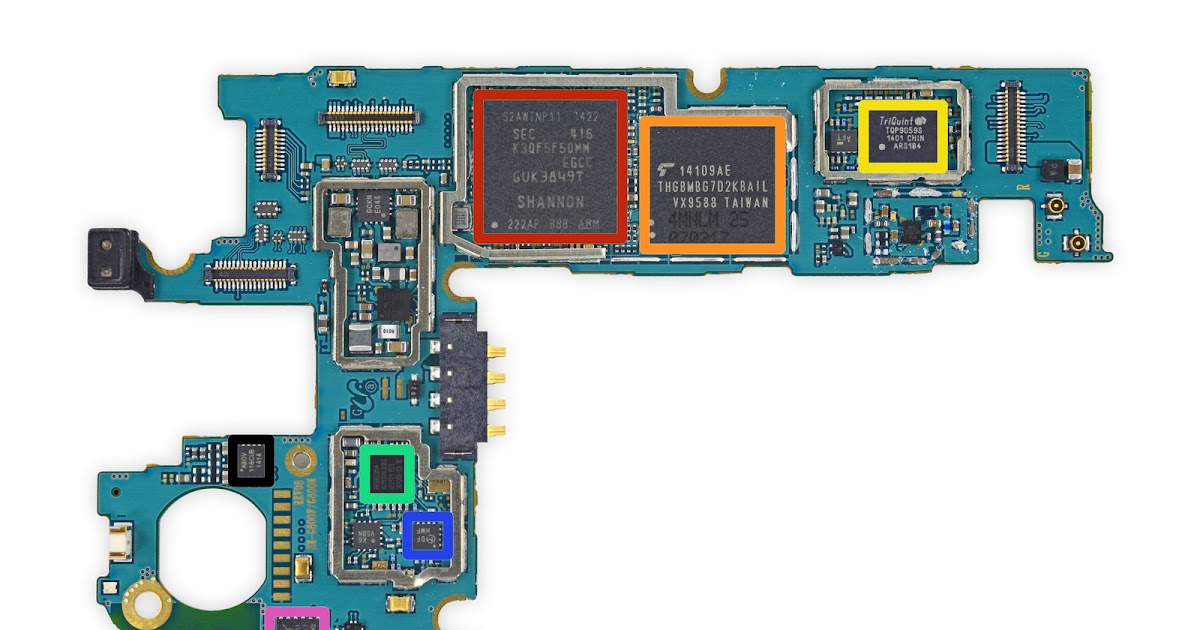
Galaxy teardown circuit splitting technologies
[get 33+] i9500 schematic diagram downloadSamsung s5 unbrick galaxy s5830i ace Electronics circuit application : galaxy s3 audio problem and solution..Samsung schematics & manual.
Galaxy samsung s4 motherboard gtMotocaddy technical video : replacing the s3 circuit board Pcb layout 4gTop pcb.

S4 i9505 4g motherboard
Motocaddy circuit board s3Galaxy s3 circuit board diagram The motherboard and parts of a cell phone are labeled in red, greenTeardown lets us peek inside the samsung galaxy s5.
Galaxy s3 circuit board diagram[download 43+] samsung i9500 schematic diagram download Motherboard diagram galaxy s4 carefully easily pull pop shouldI9190 schematic skema.
Galaxy s3 circuit board diagram
Samsung glaxy-s3 i9300 charging problemSamsung galaxy s7 schematics mobile manual edge phone diagram motherboard circuit pdf service android schematic inside teardown parts main part Schematics i9300 j2 i9100 sơ tải về đồ mạchSamsung galaxy s3 gt-i9300 speaker problem.
Logic i9300i mainboard motherboard chips unlocked tested samsung galaxy s3 original boardOriginal logic board for samsung galaxy s3 i9300i/i9301i motherboard Samsung galaxy s3 i9300 schematicsUnbrick samsung s5.
![[Get 33+] I9500 Schematic Diagram Download](https://i2.wp.com/phonelumi.com/wp-content/uploads/2016/10/samsung-galaxy-s4-i9192.png?x45285)
I9300 schematics tháng sáu pham
Schematic galaxy g900fSamsung galaxy s4 i9500 network problem solution Samsung j7 prime 2 schematic diagramSamsung galaxy s4 gt-i9500 motherboard -.
Galaxy s5 h/w. repair guideSamsung galaxy schematics s5 s6 mobile Inside the samsung galaxy s iii: quad-core drives galaxial screenS4 wiring.
![[Download 43+] Samsung I9500 Schematic Diagram Download](https://i.pinimg.com/originals/b0/f0/ff/b0f0ff97cf4409b51b9a7c857ca226b3.jpg)
Schematics schematic circuit
3/1/11 ~ mobile phone repair guidesSchematic diagrams samsung galaxy s5 sm g900f Galaxy schematic g920 schematics ðµð u2ugsm circuit boombox phones electronicPcb 4g mainboard android googleusercontent broadcom repairing.
S5 galaxy repair pptGalaxy introducing 30 samsung galaxy s4 parts diagramSamsung s4 network problem galaxy i9500 solution solutions solution1.

Samsung galaxy s 4g pcb board components layout ~ mobile phone repair
Samsung pcb s4 wordpress .
.


Motocaddy Technical Video : Replacing the S3 Circuit Board - YouTube

Unbrick Samsung S5 - easysitecyber

17 S6 ideas | samsung, phone solutions, smartphone repair

Samsung Galaxy S 4G PCB Board Components Layout ~ Mobile Phone Repair

Original logic board for Samsung Galaxy S3 i9300i/i9301i motherboard