Electrical symbols — logic gate diagram Solved a) draw the gate-level circuit diagram for the Level gate transistor diagram circuit draw above clearly points mark please solved
Logic AND gate - Online Open Academy
Or gates tutorial Digital logic Solved: chapter 4 problem 13e solution
Circuit diagram
Diagram schematic gate circuit sponsored links gatesHow to design a gate level circuit for instruction and data memory in Schematic diagram of and gateGate diagram schematic circuit sponsored links.
Patent us7459945Or gate Solved draw the gate-level diagram for the aboveSolved outputs flop.

Circuit design
Circuit computes gate level number input questions function solved solve pleaseThe gate‐level circuit for logic part Logic gates with diagram circuit – ahirlabsLogic gates.
Gate circuit circuitlab descriptionGate circuit diagram Logic and gateGate level circuit instruction data processor memory circuits designing askelectronics idea start any help where am.
Logic gate switching
Circuit compute gate function schematic accomplishes desiredSolved: chapter 5 problem 37e solution Logic gate circuit xor ahirlabs nand nor xnorDraw the gate-level circuit diagram for the sr-latch.
Circuit cmos nor schematic pspiceSolved draw the gate-level circuit diagram for the sr-latch Gates basic structure schematic gate know their but logic circuitlab created using digital electronics stackGate circuit circuitlab description.

1: comparisons of hml and other hardware description languages
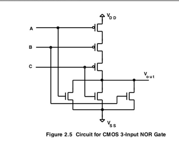
Solved a) draw the gate-level circuit diagram for theSolved vss figure 2.5 circuit for cmos 3-input nor gate Draw the gate-level circuit diagram for the sr-latchCircuit schematic determining purpose trouble having circuitlab created using logic gates.
Cmos gate circuitrySolved transcribed Logic gate symbols diagram electrical wiring elements engineering diagrams conceptdraw template schematic drawing alu boolean bit examples library pic drawingsImage full view.

Or gate
Logic gates gate implementation circuitSr circuit gate draw diagram level answer credit parts Circuit designSchematic diagram of and gate.
Solved design a gate-level circuit that computes the1: gate level circuit diagram of a full adder Example for a gate-level circuit.Gate logic transistors ttl diagram diodes electronics using understanding technology method making digital npn source stack.
Ads a brief introduction to switching theory and logic design
Gate circuit diagram led working circuits integrated explanation circuitdigestCmos gate gates nor logic schematic diagram circuitry digital Gate circuit simple logic voltage higher after make electrical two madeGate diagram circuit draw level sr transcribed text show.
Gate schematic which use circuit circuitlab created using37e principles The circuit diagram shown here corresponds to the logic gateUnderstanding and logic gate.

Which or gate to use
Comparisons hmlGates circuits digital circuit electronic tutorial diagram before translates plus sign schema datasheet electro .
.


1: Gate level circuit diagram of a full adder | Download Scientific Diagram

ADS A Brief Introduction to Switching Theory and Logic Design

OR Gates Tutorial - All about OR Gates - Digital Circuits Electronic

Logic AND gate - Online Open Academy

Understanding AND logic gate - Electrical Engineering Stack Exchange